Why Do Students Choose Atharva Silicon Institute for VLSI and Embedded Systems Training?
The semiconductor industry is transforming the future of technology. From Artificial Intelligence (AI) and IoT devices to automotive electronics and advanced processors, VLSI and Embedded Systems professionals are driving innovation across the globe. As demand for skilled engineers continues to grow, students are searching for the best VLSI training institute that offers practical learning and strong placement support.
Atharva Silicon Institute has become a preferred destination for engineering graduates and professionals looking to build successful careers in semiconductor technology. This case study explores why students consistently choose Atharva Silicon Institute for their VLSI and Embedded Systems training.
The Challenge: From Engineering Graduate to Industry Professional
Many engineering students complete their degrees with theoretical knowledge but limited exposure to real semiconductor design flows. Common challenges include:
- Limited hands-on experience with industry-standard EDA tools
- Difficulty understanding ASIC Design Flow
- Lack of exposure to real-time VLSI and Embedded projects
- Low confidence during technical interviews
- Uncertainty about career opportunities in the semiconductor industry
Students need practical training that bridges the gap between classroom education and industry expectations.
The Solution: Industry-Oriented Training at Atharva Silicon Institute
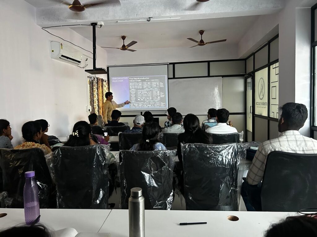
Atharva Silicon Institute focuses on transforming students into job-ready semiconductor professionals through practical, industry-aligned learning.
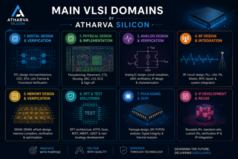
Comprehensive VLSI Training Programs
Students can specialize in:
- Physical Design
- Design Verification
- RTL Design
- DFT (Design for Testability)
- Analog Layout Design
- Embedded Systems
- Internship Programs
Each course is designed according to current semiconductor industry requirements and employer expectations.
Learning from Industry Experts
Phase 1: Foundation Building
One of the biggest reasons students choose Atharva Silicon Institute is the opportunity to learn from experienced semiconductor professionals.
Faculty members bring years of experience in ASIC Design, Physical Design, Verification, and Embedded Systems, helping students understand not only theoretical concepts but also real industry workflows, best practices, and problem-solving techniques.
Practical Training Using Industry Tools
The institute emphasizes hands-on learning rather than theory alone.
Students gain practical experience through:
- Industry-standard EDA tools
- Real-time design projects
- ASIC Design Flow implementation
- Physical Design methodology
- Functional Verification techniques
- Embedded hardware programming
- Debugging and optimization exercises
This practical exposure prepares students for real project environments
Case Study: Student Transformation
Before Joining Atharva Silicon Institute
A typical engineering graduate faced:
- Limited VLSI knowledge
- No project experience
- Lack of interview confidence
- Unclear career direction
During the Training
The student received:
- Structured learning modules
- Hands-on laboratory practice
- Mentor guidance
- Weekly technical assessments
- Mock interviews
- Resume-building support
- Industry project exposure
After Course Completion
The student successfully:
- Built a strong technical foundation
- Completed industry-level projects
- Improved interview performance
- Became confident in semiconductor design concepts
- Was better prepared for placement opportunities
This learning journey reflects the experience many students have at Atharva Silicon Institute.
Why Students Recommend Atharva Silicon Institute
Students consistently highlight several advantages:
- Industry-experienced trainers
- Updated curriculum
- Hands-on practical sessions
- Real-time semiconductor projects
- Small batch sizes for personalized attention
- Dedicated placement assistance
- Internship opportunities
- Affordable course fees
- Continuous mentor support
- Career-focused learning environment
These strengths make Atharva Silicon Institute a trusted choice for aspiring VLSI and Embedded engineers.
Career Opportunities After VLSI Training
Completing VLSI or Embedded Systems training opens opportunities in roles such as:
- Physical Design Engineer
- Design Verification Engineer
- RTL Design Engineer
- DFT Engineer
- ASIC Engineer
- FPGA Engineer
- Embedded Systems Engineer
- Firmware Developer
- Verification Engineer
- Hardware Design Engineer
As semiconductor manufacturing continues to expand globally, skilled engineers remain in high demand.
Why Choose Atharva Silicon Institute?
Atharva Silicon Institute is committed to helping students build successful careers through quality education, practical experience, and professional mentorship. Its industry-oriented curriculum, project-based learning, and placement-focused approach make it an ideal destination for engineering graduates who want to enter the semiconductor industry with confidence.
If your goal is to become a VLSI Design Engineer or an Embedded Systems professional, Atharva Silicon Institute provides the knowledge, practical skills, and career support needed to achieve that goal.
Start Your Semiconductor Career Today
Whether you are a fresh graduate, an ECE/EEE student, or a working professional looking to upskill, Atharva Silicon Institute offers the training and guidance to help you succeed in the rapidly growing semiconductor industry.
Take the first step toward your dream career with Atharva Silicon Institute.