The semiconductor industry is rapidly expanding, and the demand for skilled VLSI engineers is at an all-time high. If you are looking to build a successful career in chip design, now is the perfect time to enroll in the Physical Design & Logical Design Courses at Atharva Silicon Institute and avail an exclusive 15% Discount Offer.
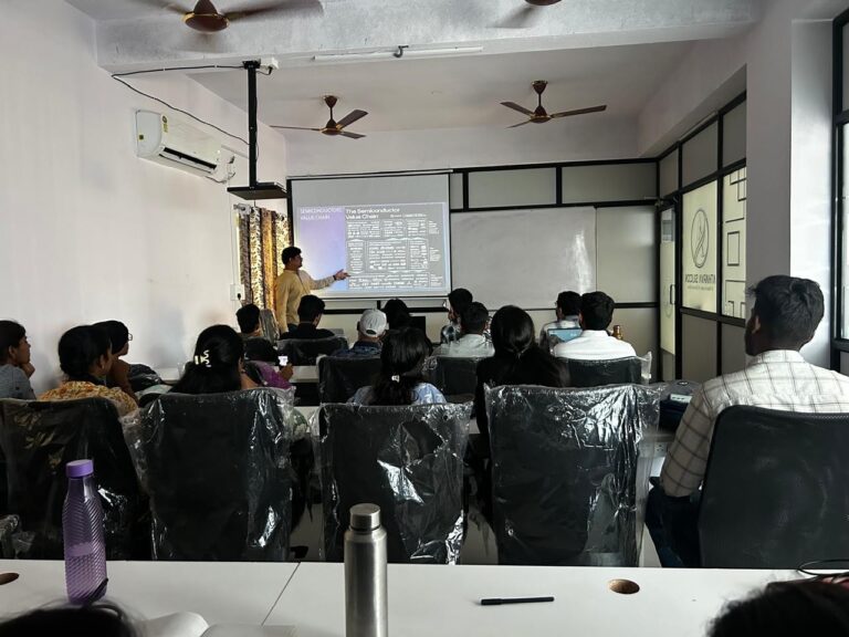
Whether you are an ECE graduate, fresher, working professional, or engineering student, these industry-oriented VLSI courses are designed to provide practical exposure, real-time projects, and placement-focused training.
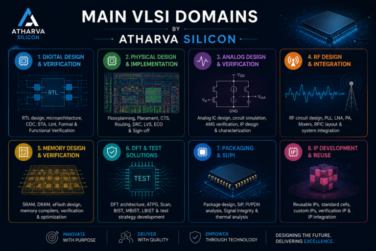
Physical Design is the backend implementation stage of VLSI chip design where the logical circuit is converted into a physical layout ready for fabrication.
The Physical Design flow includes:
- Floorplanning
- Power Planning
- Placement
- Clock Tree Synthesis (CTS)
- Routing
- Static Timing Analysis (STA)
- Signoff Verification
- GDSII Generation
Modern semiconductor companies require engineers with expertise in advanced Physical Design methodologies to develop high-performance and low-power chips.


Logical Design, also called RTL Design, is the frontend stage of VLSI design where digital circuits are designed using Hardware Description Languages such as Verilog and SystemVerilog.
Students learn:
- Digital Electronics Fundamentals
- Verilog HDL
- RTL Coding
- FSM Design
- Synthesis Concepts
- Timing Constraints
- Low Power Design Basics
- Functional Simulation
Logical Design engineers work closely with Verification and Physical Design teams to create efficient semiconductor architectures.
- Industry-Oriented Training
The course is designed according to current semiconductor industry requirements and includes practical learning using industry-standard flows.
-
Experienced Mentors
Students learn from professionals with real-time VLSI industry experience in ASIC Design and Semiconductor Engineering.
-
Practical implementation of:
- RTL to GDSII Flow
- Timing Closure
- Synthesis Flow
- STA Analysis
- Chip Design Projects
-
Students receive:
- Resume Building
- Mock Interviews
- Technical Guidance
- Placement Support
- Online VLSI Training
- Offline Classroom Training
- Weekend Batches
- Fast-Track Programs
Physical Design Course Modules
- Unix & TCL
- CMOS Technology
- Floorplanning
- Placement Optimization
- CTS
- Routing
- STA
- IR Drop & Power Analysis
- Signoff Checks
- Physical Verification
Logical Design Course Modules
- Digital Design Concepts
- Verilog HDL
- RTL Coding
- FSM Design
- Synthesis
- Timing Analysis
- Lint & CDC Basics
- FPGA Fundamentals
Career Opportunities After Completing the Course
After successful training, students can apply for roles such as:
- Physical Design Engineer
- RTL Design Engineer
- ASIC Design Engineer
- STA Engineer
- FPGA Engineer
- Backend VLSI Engineer
- Frontend Design Engineer
- Verification Engineer
Top semiconductor companies hiring in these domains include Intel, Qualcomm, NVIDIA, AMD, Synopsys, Cadence, Samsung, and MediaTek.
Final Thoughts
The future of semiconductor technology is expanding rapidly, and companies are actively searching for skilled VLSI professionals with practical knowledge in Physical Design and Logical Design.
Joining the Physical Design & Logical Design Course at Atharva Silicon Institute can help students gain industry-ready skills, hands-on project exposure, and career opportunities in the growing semiconductor industry.
If you are searching for the best VLSI training institute in Hyderabad, now is the right time to start your journey into semiconductor chip design.
Start Your VLSI Career Today
The semiconductor industry offers excellent career growth and high-paying opportunities. Gain industry-ready skills with the Physical Design & Logical Design Courses at Atharva Silicon Institute and take advantage of the 15% OFF Limited-Time Offer.