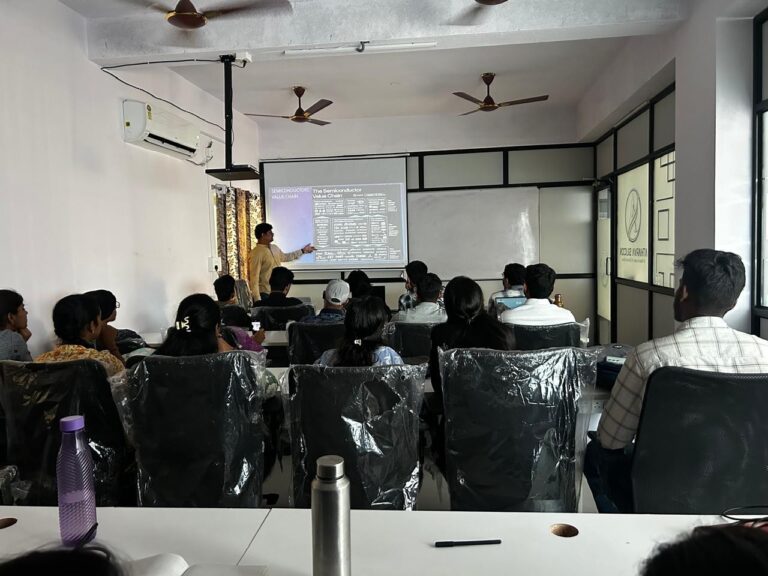
WHAT IS VLSI
VLSI (Very Large Scale Integration) is the process of designing and manufacturing integrated circuits (chips) that contain millions or billions of transistors on a single silicon chip. VLSI technology is used in smartphones, laptops, processors, memory chips, automobiles, networking equipment, and AI accelerators.
WHY IS VLSI IMPORTANT?
- Makes electronic devices smaller and faster.
- Reduces power consumption.
- Increases computing performance.
- Enables modern technologies such as AI, 5G, IoT, and cloud computing.
- Reduces overall system cost.

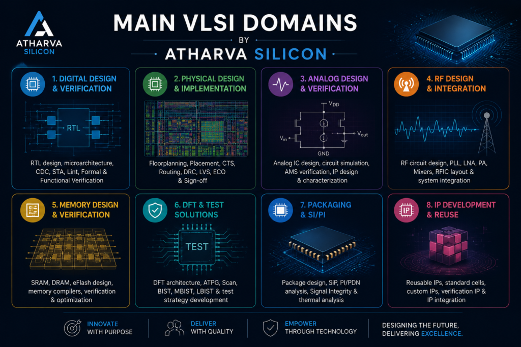
MAIN VLSI DOMAINS
- 1.(Register level Transfer)RTL DESIGN (Front-End Design)
RTL engineers convert product requirements into digital hardware using Verilog or SystemVerilog. They design modules such as processors, controllers, memory interfaces, and communication blocks.
Output: RTL Code.
- 2. FUNCTIONAL VERIFICATION
Verification engineers ensure that the RTL design behaves exactly as intended. They create testbenches, generate test cases, and find bugs before manufacturing.
Output: Verified RTL Design.
- 3. DFT (DESIGN FOR TEST)
DFT engineers add special structures such as Scan Chains, MBIST, and JTAG so that manufactured chips can be tested for defects.
Output: Testable Design.
- 4. LOGIC SYNTHESIS
Synthesis converts RTL code into a gate-level netlist using standard-cell libraries. This is the bridge between front-end and back-end design.
Output: Gate-Level Netlist.
- 5. PHYSICAL DESIGN
Physical Design engineers convert the netlist into a physical chip layout.
Main Steps:
• Floorplanning – Arranging major blocks.
• Power Planning – Creating power and ground networks.
• Placement – Positioning standard cells.
• CTS – Building the clock network.
• Routing – Connecting all cells using metal layers.
• Signoff – Final quality checks.
Output: Physical Layout.
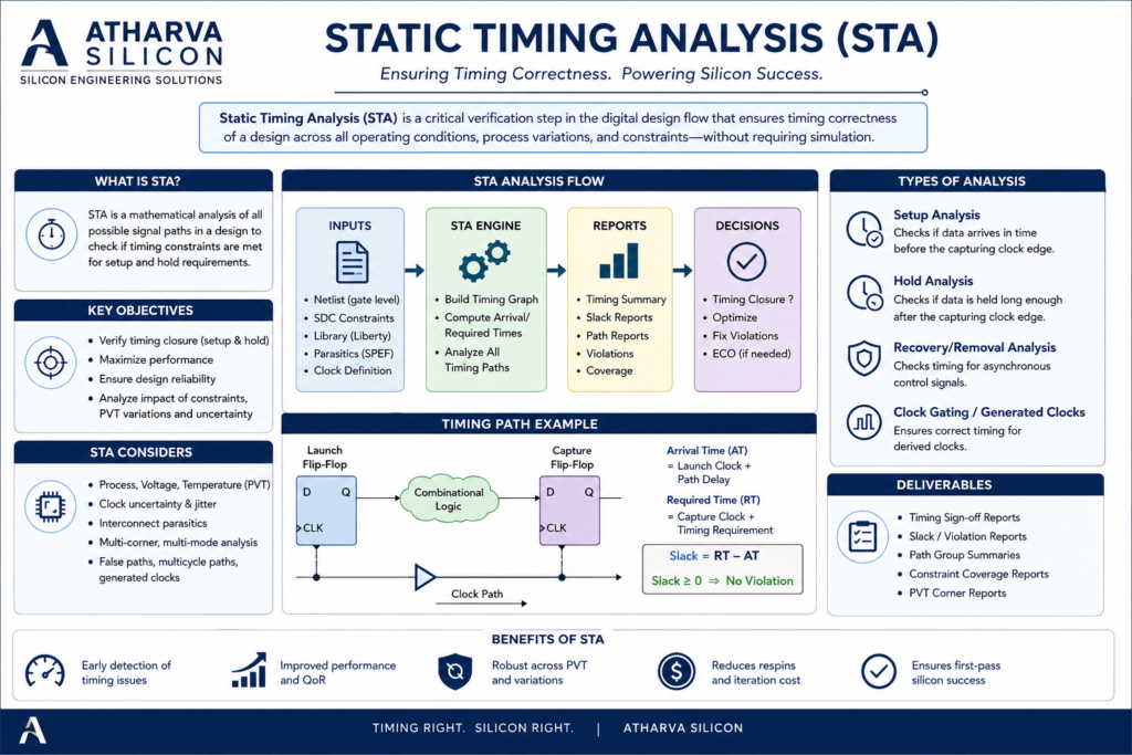
- 6. STATIC TIMING ANALYSIS (STA)
STA engineers check whether all signals meet timing requirements. They analyze setup, hold, clock skew, and timing violations without simulation.
Output: Timing-Clean Design.
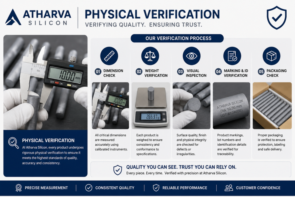
- 7. PHYSICAL VERIFICATION
This domain ensures the layout can be manufactured correctly.
Checks include:
• DRC (Design Rule Check)
• LVS (Layout Versus Schematic)
• ERC (Electrical Rule Check)
Output: Manufacturing-Clean Layout.
- 8. ANALOG / MIXED-SIGNAL DESIGN
Engineers design circuits that process real-world signals such as PLLs, ADCs, DACs, amplifiers, and voltage regulators.
Output: Analog Circuit Design.
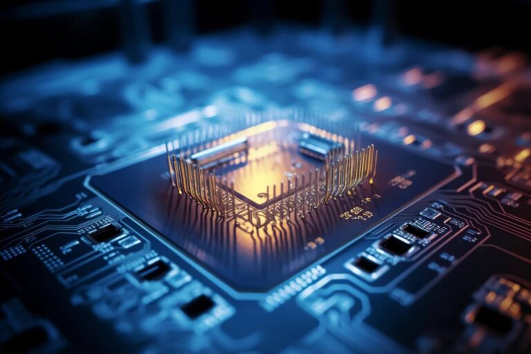
- 9. SEMICONDUCTOR MANUFACTURING
After design completion, the layout is sent to a foundry where silicon wafers are fabricated into actual chips.
Examples: TSMC, Samsung Foundry, Intel Foundry.
Output: Silicon Chip.
COMPLETE VLSI FLOW
Specification
- RTL Design
- Functional Verification
- DFT
- Logic Synthesis
- Physical Design
- STA
- Physical Verification
- Fabrication
- Final Chip
COMMON CAREER ROLES
- RTL Design Engineer
- Verification Engineer
- DFT Engineer
- Physical Design Engineer
- Synthesis & STA Engineer
- Physical Verification Engineer
- Analog Design Engineer
- CAD/EDA Engineer
- EMIR Engineer
SUMMARY
VLSI is the technology behind modern electronic devices. Each domain has a specific responsibility, and all domains work together to transform an idea into a manufactured semiconductor chip.