
Physical Design Course – New Batch Starting April 13th
Atharva Silicon Institute
Are you looking to build a successful career in the Semiconductor / VLSI industry? Atharva Silicon Institute is launching a new batch of the Physical Design Course starting on April 13th, designed to train students and professionals with industry-ready skills in VLSI Physical Design.
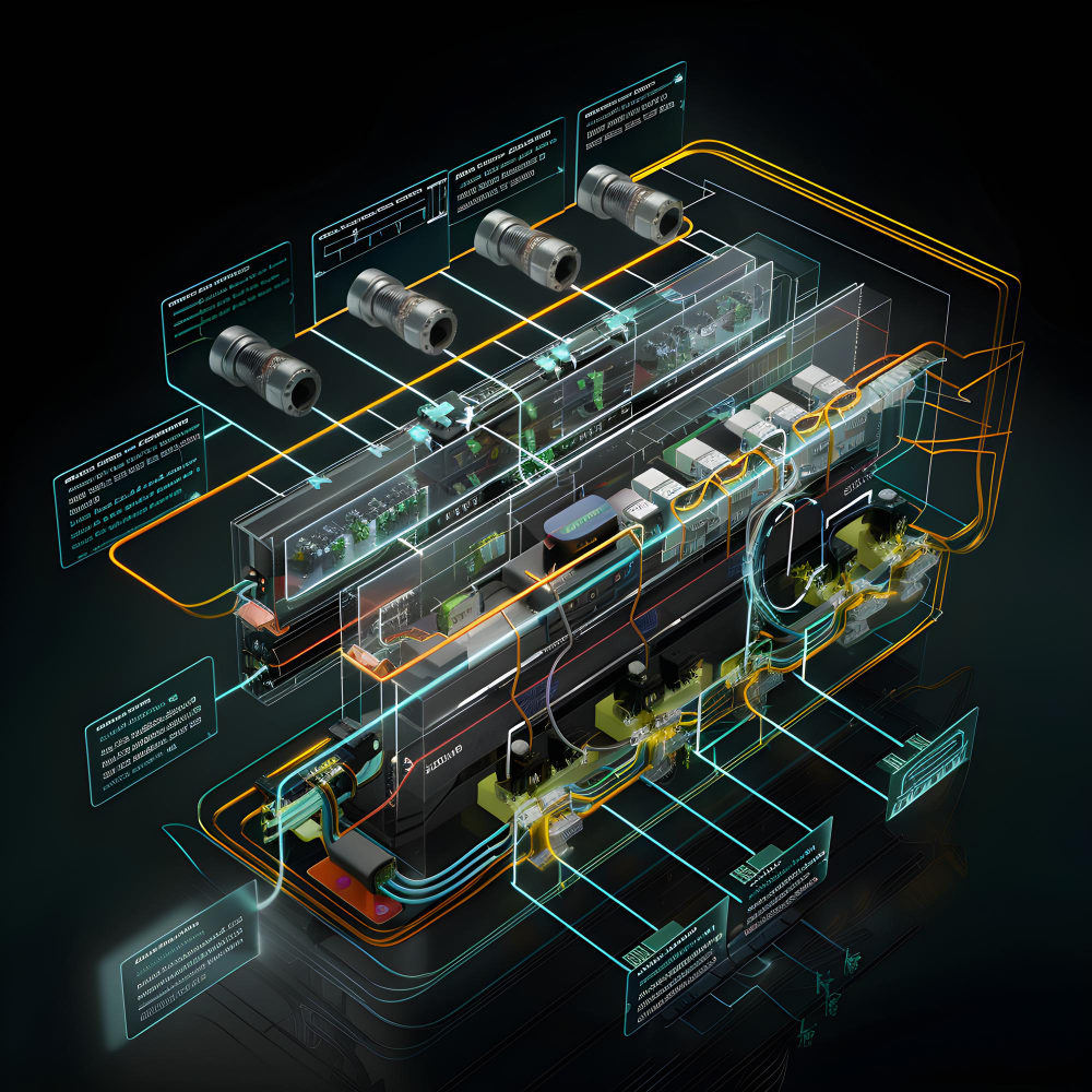
This course provides complete hands-on training from RTL to GDSII flow, enabling learners to understand real-time chip design implementation used in leading semiconductor companies.
Our expert mentors guide students through practical tools, real industry design flow, and advanced concepts required to become a skilled VLSI Physical Design Engineer.
Physical Design Course Curriculum
- RTL to GDS Flow
- Understand the complete ASIC design flow from RTL design to final chip tape-out, including the implementation stages used in modern semiconductor companies.
- Floorplanning
- Learn how to design efficient chip layouts by defining die size, macro placement, power planning, and routing resources.
- Synthesis
- Convert RTL code into optimized gate-level netlists while considering timing, area, and power constraints.
- Placement
- Master the techniques of placing standard cells on the chip to achieve optimal performance and minimal congestion.
- Clock Tree Synthesis (CTS)
- Design balanced clock networks to ensure minimal skew, low latency, and reliable clock distribution across the chip.
- Routing
- Learn global and detailed routing techniques to connect all components while meeting design rules and timing requirements.
Sign-off and Verification Modules
- Sign-off Checks
- Understand the final verification stages required before chip manufacturing.
- LEC (Logical Equivalence Check)
- Verify that the synthesized netlist matches the RTL functionality.
- STA (Static Timing Analysis)
- Analyze timing paths to ensure the design meets required performance constraints.
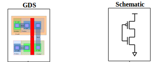
- Physical Verification (PV)
- Learn industry-standard checks such as:
- DRC (Design Rule Check)
- LVS (Layout vs Schematic)
- These checks ensure the design is manufacturable and functionally correct.
- IR Drop Analysis
- Understand power integrity analysis to detect voltage drops and ensure stable chip operation.
- Low Power Techniques
- Learn power optimization methods used in modern chip designs including low-power architecture and design methodologies.
Why Choose Atharva Silicon Institute?
- Industry-oriented RTL to GDSII training
- Experienced semiconductor professionals as trainers
- Hands-on tool exposure
- Real-time design flow understanding
- Career guidance and industry ecosystem support
Atharva Silicon aims to bridge the gap between academic learning and semiconductor industry requirements by building a strong ecosystem of training, design services, and industry exposure.
Enroll Now – Limited Seats Available
The Physical Design Course Batch starting on April 13th is open for ECE, EEE, and VLSI aspirants who want to start their career in the semiconductor industry.
Take the first step towards becoming a VLSI Physical Design Engineer with Atharva Silicon Institute.