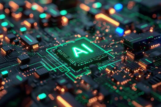
The rapid advancement of Artificial Intelligence (AI) is revolutionizing industries worldwide, and the VLSI semiconductor industry is no exception. From chip design automation to intelligent verification and manufacturing optimization, AI is reshaping how modern integrated circuits are developed.
At Atharva Silicon Institute, we prepare aspiring engineers to adapt to this transformation by equipping them with cutting-edge skills in VLSI design and AI-driven semiconductor technologies.
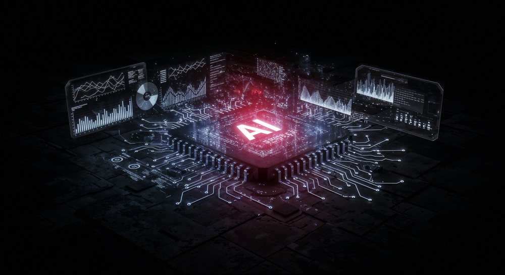
Artificial Intelligence in VLSI refers to the integration of machine learning algorithms, deep learning models, and data-driven techniques into the semiconductor design and manufacturing process.
AI helps engineers:
- Automate complex design workflows
- Optimize chip performance and power
- Reduce time-to-market
- Improve accuracy in verification and testing

- AI in Chip Design Automation (EDA Tools)
- AI-powered Electronic Design Automation (EDA) tools are transforming traditional design flows.
- Automated floorplanning and placement
- Intelligent routing optimization
- Faster RTL-to-GDSII flow
3. AI in Verification and Testing
Physical design is one of the most complex stages in VLSI. AI simplifies it by predicting optimal layouts.
Benefits:
-
- Reduced power consumption
- Improved timing closure
- Efficient congestion management
Verification consumes nearly 70% of the design cycle. AI drastically reduces this burden.
Applications:
- Automated test pattern generation
- Bug prediction using ML models
- Faster regression testing
SEO Keywords: AI in VLSI verification, semiconductor testing automation
AI enhances yield and quality in fabrication processes.
Key Uses:
- Defect detection using computer vision
- Predictive maintenance in fabs
- Process optimization
AI algorithms analyze vast datasets to optimize chip performance.
Advantages:
- Better PPA (Power, Performance, Area) trade-offs
- Dynamic voltage and frequency scaling
- Smart thermal management
- Reduced design cycle time
- Improved chip performance
- Lower manufacturing costs
- Enhanced design accuracy
- Faster innovation in semiconductor technology
While AI brings massive advantages, there are also challenges:
- High computational requirements
- Need for large datasets
- Complexity in AI model integration
- Skill gap in AI + VLSI expertise
The future of AI in VLSI is extremely promising:
- AI-designed chips (self-learning architectures)
- Advanced node designs (3nm, 2nm technologies)
- AI-driven hardware accelerators
- Integration with IoT, 5G, and autonomous systems
At Atharva Silicon Institute, we bridge the gap between academic knowledge and industry requirements.
Our Key Highlights:
- Industry-focused VLSI training programs
- Hands-on experience with real-time projects
- Exposure to AI-integrated chip design concepts
- Expert mentorship from industry professionals
100% skill development & interview opportunities
The integration of AI in the VLSI semiconductor industry is not just an innovation—it is a necessity for the future. Engineers who understand both AI and VLSI design will lead the next generation of semiconductor advancements.
If you are looking to build a career in this evolving domain, now is the right time to start.